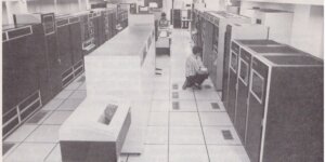


Smart memory: Godiva unit now running in a standard HP Long~s Peak Server.
Researchers at the University of Southern California have successfully integrated a next-generation “smart memory” chip into a standard HP computer.
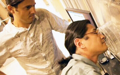
“It’s a major milestone,” said Mary Hall, co-project leader of the “Godiva” team working at USC Viterbi School of Engineering’s Information Sciences Institute. “Even though our chip has a fundamentally different architecture than the conventional hardware the HP platform was designed around, it’s working. Now we’re seeing if it will deliver the extra speed and power theory promises.”Hall, an ISI software specialist who also holds an appointment in the Viterbi School’s department of computer science, has been working on a DARPA-funded effort to improve “processor in memory” or PIM chips for more than four years.
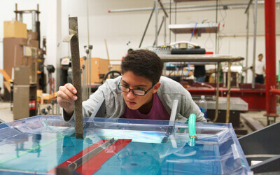
She and hardware architect Jeff Draper deployed their team’s new chips in HP Long’s Peak server memory modules. “And these modules are now functioning as designed, as part of a working computer.” HP and Rice University are also part of the project, Hall said.
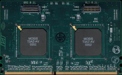
Double Down: Godiva chips as installed in the HP circuit board. Tests are now underway to determine if performance improvements match predictions.
“Computer scientists have been talking about the potential of PIM chips for most of the past decade and have released devices they call PIM chips,” said Draper, “but this is the first smart-memory device designed to support virtual addressing and capable of executing multiple threads of control.”
PIMs potentially eliminate the communication bottleneck that takes place when processing chips have to go back and forth to separate memory chips to get data for computations, and then store the results, Draper continued. A PIM chip can keep results and data in its own memory, resulting in dramatic gains in speed.
But theory has been very hard to turn into practice, the researchers say. The successful integration of the new chips into a standard computer like the Long’s Peak server marks a substantial new achievement, according to Hall and Draper.
The new device is an expanded and improved version of the product of an earlier effort by Hall, Draper and ISI Division Director John Granacki. That project, DIVA, built a 55-million transistor PIM chip that the DIVA team demonstrated in a development system July 31, 2002, at the DARPATech 2002 Symposium in Anaheim California.
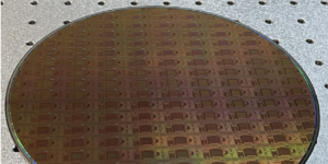
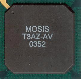
The Godiva project chip is slightly larger (56 million transistors) offers address translation and eight single-precision floating point units, and perhaps most important, contains a memory interface compatible with DDR SDRAM memory buses.
Both the DIVA and the Godiva designs are among the largest chips ever realized in academia. Both were fabricated at Taiwan Semiconductor Manufacturing Corporation (TSMC) through ISI’s MOSIS chip brokerage.
Hall, Draper and colleagues are now testing the PIM- enhanced Long’s Peak server on tasks such as multimedia, complex scientific modeling and database access. “Our calculations indicate we may get as much as an order of magnitude better performance.”
Besides Hall and Draper, the Godiva team includes ISI researchers Jacqueline Chame (Simulation, Benchmarking and Compiler), Tim Barrett (System Integration), Jeff Sondeen (VLSI), Dale Chase (System Integration), and Spundun Bhatt (programming). Many USC graduate students also contributed to this project.
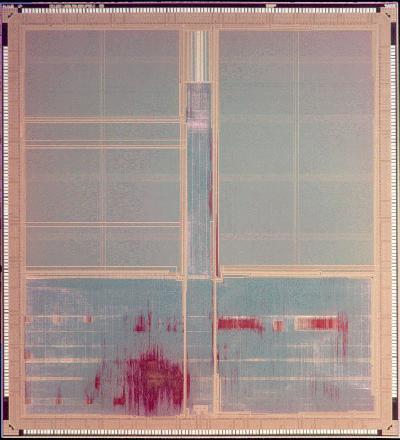
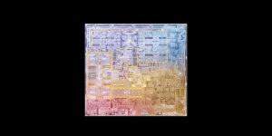
Close Up: The 56-million-transistor Godiva processor-in-memory (PIM) chip is one of the largest ever created in academia.
Published on June 24th, 2004
Last updated on August 9th, 2021