


Photo/iStock
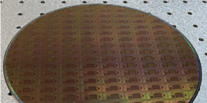
An ISI research team, led by Advanced Electronics division director John Damoulakis, is developing techniques to clearly image the smallest features in silicon integrated circuit chips at a resolution of sub-10 nanometers (10 billionths of a meter).
The goal is to capture the chip’s tiny internal wiring and transistors without distortions or deformations.
The team aims to image a single square centimeter chip within 25 days using X-rays and ptychotomography — a non-destructive tomographic method used to create detailed nanoscale 3D images of an electronic chip.
ISI’s PRISMA team is one four research groups working on the program, along with Varioscale, BAE Systems and The Massachusetts Institute of Technology (MIT).
The three-phase IARPA-funded project, dubbed the Rapid Analysis of Various Emerging Nanoelectronics (RAVEN) program, was featured in a recent article by Semiconductor Engineering.
How it works
Integrated circuits comprise dozens or more layers of nanoscale components, making it difficult for manufacturers to measure, for example, how closely a finished chip conforms to specifications.
For such examinations with existing techniques, each layer must be removed and viewed under an electron microscope, which can cause structural damage and image distortion.
By using x-ray ptychography combined with tomography instead, conducting lines and individual transistors can be rendered clearly and non-destructively.
To deal with this method’s substantial computational requirements, ISI’s PRISMA team is also developing scalable algorithms that use both machine learning and high-performance accelerators to work more efficiently using fewer resources.
Read more about the RAVEN program.
Published on August 2nd, 2017
Last updated on June 2nd, 2021