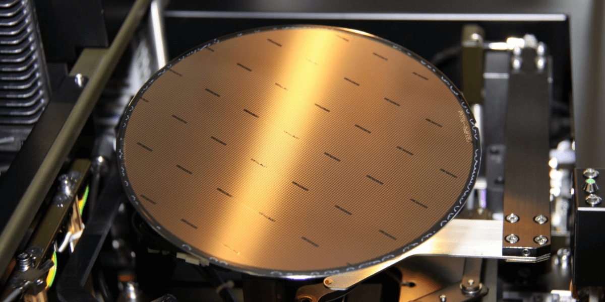
150mm GaAs Wafer Photo credit: WIN Semiconductors Corp.
LOS ANGELES (MAY 31, 2022) – The MOSIS Service of Information Sciences Institute, University of Southern California and WIN Semiconductors Corp. today announced a Memorandum of Understanding to accelerate the development of GaAs and GaN Monolithic Microwave Integrated Circuits (MMICs) with WIN Semiconductors’ GaAs and GaN process technologies. Project flows for customers to utilize The MOSIS Service to fabricate MMICs at WIN Semiconductors Corp will be released.
The collaboration combines the MOSIS world-class semiconductor design support and manufacturing expertise, including Multi-Project Wafer (MPW) runs, and WIN Semiconductors’ industry-leading manufacturing technologies for high-speed devices utilizing III-V compound semiconductors including Gallium Arsenide (GaAs) and Gallium Nitride (GaN), and prototype packaging technologies. With this collaboration universities, research organizations, and industry organizations will have access to an extensive portfolio of heterojunction bipolar transistor (HBT), Pseudomorphic high-electron-mobility transistor (pHEMT) and RF Gallium Nitride High Electron Mobility Transistor (GaN HEMT) technology platforms to develop new high performance MMIC designs. The collaboration lays the foundation for innovative, reliable, and efficient design and prototyping flows through the MPW projects with The MOSIS Service and WIN Semiconductors.
“This is a new and important capability for The MOSIS Service to provide access and support to non-silicon wafer fabrication processes with the microelectronics community.” said Craig Knoblock, Executive Director of Information Sciences Institute. “For the first time, the U.S. Government, R&D laboratories, companies, and academia will have access to WIN Semiconductors’ portfolio of III-V compound semiconductor processes with MOSIS’ legacy design and manufacturing service capabilities. We are confident that this collaboration will significantly advance microelectronics R&D and accelerate the development of advanced GaAs and GaN MMICs.”
“We are excited to launch this initiative with WIN Semiconductors” said Lifu Chang, Director of The MOSIS Service. “WIN Semiconductors is the world leader in the pure-play compound semiconductor foundry space and offers a comprehensive portfolio of III-V technologies. These III-V foundry technologies require a higher level of design-technology interplay compared to silicon technologies. Our MOSIS experience provides a platform for tightly coupled and efficient design and manufacturing flows, to support universities and design companies interested in high-performance front-end applications.”
Knoblock echoed this statement, “There are serious concerns with the access to wide varieties of semiconductor processes and design support for universities and corporations in the US, in the context of worldwide competition and wafer supply constraints. The MOSIS Service is positioned to contribute to the resolution. The addition of GaAs and GaN technologies is necessary, and we will push hard in this direction.”
WIN Semiconductors’ Senior Vice President of Technology and Strategic Business Development, David Danzilio, said, “The collaboration between WIN Semiconductors and The MOSIS Service creates a new platform for many new users to access WIN’s market leading compound semiconductor technologies.” Danzilio pointed out, “We are building a robust project framework with MOSIS’ Team. I expect to attract and enable many customers that have been interested but need the level of technical support that MOSIS can provide. WIN is the largest pure-play compound semiconductor foundry, and we welcome the new customer engagements provided by The MOSIS Service”.
About the Technology
The WIN-MOSIS collaboration leverages the extensive III-V technology and manufacturing expertise of WIN Semiconductors Corp. Compound semiconductors are an enabling technology used in satellite communications, optoelectronic components, wireless and fiber optic networks, and the mobile devices connecting billions of people across the world. With their superior electron transport characteristics, GaAs and GaN devices outperform silicon technologies in critical front-end applications and provide higher linearity, efficiency, output power and lower noise figure. The collaboration is focused on the development of new Monolithic Microwave Integrated Circuits (MMICs) and the technologies included in this program support amplifier designs and integrated front ends operating from 100 MHz to 175 GHz. These technology platforms incorporate various integration options including multiple metal layers, logic interfaces, compact ESD protection, copper-pilar bumps and through-chip RF transitions. WINs proven GaAs and GaN technologies support large scale chip manufacturing, delivering billions of MMICs annually to WIN’s customers. The collaboration will also provide access to prototype QFN packaging technologies from WIN Semiconductors.
Published on May 31st, 2022
Last updated on May 16th, 2024
