

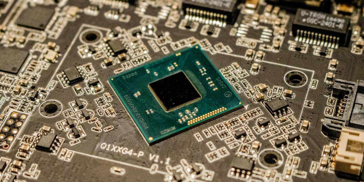
USC Viterbi researchers are investigating new materials to produce the high-quality chips that we will require for our future data needs. Image/Jeremy Waterhouse, Pexels.
The semiconductor industry is facing a race against time to develop advanced materials with unique electronic properties to make chips that can handle our needs in the future of massive data. As the complexity of the chips increases, there is a greater need for new electronic materials and precise techniques to grow them with unprecedented control.
Recently, materials scientists have been exploring new electronic materials known as chalcogenides, which have the unique electronic and photonic properties necessary for the high-performance devices of the future.
These materials need to be synthesized in the form of crystalline thin films to realize these properties. However, growing the films to a high quality without defects is particularly challenging. If the chalcogenides contain sulfur, the growth challenges are further amplified because precursor materials for sulfur are toxic, reactive and difficult to control.
Ph.D. researcher in the Mork Family Department of Chemical Engineering and Materials Science, Mythili Surendran, and her collaborators in USC Viterbi’s Laboratory for Complex Materials and Devices have now devised a novel technique to grow these thin film materials safely and to a high standard. Their work has been published in Advanced Materials.
Under the leadership of Jayakanth Ravichandran — the Philip and Cayley MacDonald Endowed Early Career Chair and associate professor of chemical engineering and materials science and electrical and computer engineering — Surendran and her collaborators have been investigating how to grow sulfur-containing materials in thin film form.

Mythili Surendran. Image/supplied.
“Sulfide thin film growth typically uses precursors such as hydrogen sulfide (H₂S) that are difficult to control and often corrosive. This makes the process particularly challenging as it needs additional safety precautions and training,” Surendran said.
The team needed to think outside the box to come up with a method to develop high-quality films using non-toxic materials while maintaining the film’s flawless intricate structure. They introduced a new technique called hybrid pulsed laser deposition, harnessing a non-corrosive organosulfur compound as the sulfur source for thin film growth.
In pulsed laser deposition, a high-energy ultraviolet laser evaporates the sulfide target, creating a plume that travels in a vacuum chamber and is deposited onto a substrate surface in film form. A sulfur-containing gas needs to be used to accurately control the composition of the film. Organosulfur precursors are often utilized in common thin film growth techniques such as chemical vapor deposition. However, this is the first time these are being employed in a pulsed laser deposition process as a sulfur source.
“We are switching to an organic precursor which has sulfur in it. It’s efficient, as it has optimal vapor pressure and also, people don’t have to worry about using hydrogen sulfide in their chambers. You can also control it precisely and decompose it at much lower temperatures. This is an important need for the semiconductor industry as we have to grow these materials at low temperatures to integrate these devices directly on our current silicon-based electronic chips without degrading those chips,” Surendran said.
Surendran said the team’s approach has proven remarkably effective in growing high-quality epitaxial chalcogenide films (where thin film grows in well-defined orientations with respect to the substrate) that are superior in structure to the output from previous methods.
“It’s a much more efficient process than using hydrogen sulfide. Our approach enhances every aspect of the growth – the environmental aspect, reduction in cost and temperature, and ease of handling. More importantly, hybrid pulsed laser deposition can be easily extended to grow other materials in the chalcogenide family, like selenides and tellurides, just by changing the precursor,” Surendran said.
The team is now investigating how this technique can be improved, scaled up, and applied to grow thin films of different material classes to a similarly high standard. Surendran said that while sulfide thin film materials were still in their infancy, it was exciting to work towards solving some aspects of the synthesis challenges of this class of materials. She said hybrid pulsed laser deposition could develop into a viable route to synthesize vapor pressure mismatched materials broadly. These results will eventually lead to growing high-quality electronic-grade chalcogenides for future technology.
The work was funded by an Air Force Office of Research DURIP Grant and by the Army Research Office.
Published on June 19th, 2024
Last updated on August 13th, 2024