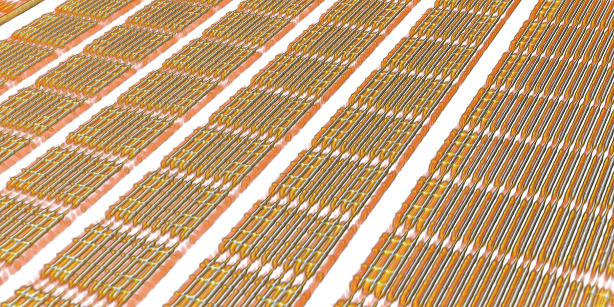
3D x-ray imaging of Integrated Circuits with a record 4nm resolution. Image credit: Tomas Aidukas, Paul Scherrer Institute
Guaranteeing that computer chips, consisting of billions of interconnected transistors, are manufactured without defects is a challenge. But how does one determine if a chip is compromised? Now, an updated technique co-developed by researchers at the Paul Scherrer Institute in Switzerland and by researchers at the USC Viterbi School of Engineering would image chips in 3D non-destructively to ensure that they haven’t been altered and that they are manufactured to design specifications. This new type of metrology promises efficient identification of subtle manufacturing defects that are difficult to identify using other techniques.
Hardware security is a critical issue. Anthony F. J. Levi, Professor of Electrical and Computer Engineering and Physics and Astronomy at USC, and co- author of the Nature study, “High-performance 4 nm resolution X-ray tomography using burst ptychography” , says the team’s results “include dramatic improvements in non-destructive imaging of advanced integrated circuits.”
The team had previously applied ptychographic X-ray laminography, a technique that utilizes X-rays from a synchrotron to illuminate a small region of a rotating chip, at an angle of 61 degrees with respect to the normal of the chip plane. The resulting diffraction patterns were measured with a photon-counting detector array. The data were then used to generate high-resolution slice images of the chip, from which 3-D renderings are created.
Once a 3-D image is generated, it can be compared with the original design, thus providing a type of forensics that helps ensure chips are manufactured correctly and that they meet design specifications.
With this newly improved method, it is possible using X-rays to also validate the integrity of computer chips at an even finer level. Levi says that 3-D X-ray imaging of metal interconnects and transistors with a record 4nm resolution is feasible. In addition, there is a 10x increase in depth of field and a much faster acquisition rate.
Previously, resolutions were limited by mechanical vibrations. Such limitations have now been dramatically reduced by the current approach, which is based on changing the way the X-ray detector hardware is used and on improving imaging algorithms. In essence this approach is similar to that used to remove distortion from shaking in regular cameras.
Levi says, “With a few upgrades, including an increase in X-ray flux, there is now no real barrier to a future in which 3-D imaging of chips at sub-nm resolution, the reverse engineering of an integrated circuit non-destructively, and its manufacture, can all be offered as a service.”
Published on August 16th, 2024
Last updated on September 6th, 2024
