

Engineering and Designing Novel Materials & Production Processes
Building on Materials Science
 Our ability to create tools and to fabricate and assemble beneficial combinations of materials has accelerated human progress and enhanced the quality of human life. As our knowledge of materials has progressed to the atomic and subatomic level, our need and ability to manipulate, control and model processes and materials at a comparable dimension has increased, resulting in unprecedented advances in the ability to control materials and devices at the micrometer and nanometer scale. Electronic, photonic, mechanical and microfluidic systems benefit from nanofabrication of smaller, denser electronic circuits with greater computational capability and system complexity and engineered nanoscale materials that are robust and highly functional. Future progress will be achieved through further scaling of these technologies to achieve atomistic scaled processes for the assembly and manufacturing of functional materials and devices. Impeding this progress are limits imposed by the atomistic nature of the materials themselves. Electronic systems are approaching the limits of our current technology for assembling electronic devices into circuits with greater capability and lower power dissipation. Atomic scaled defects impose limits on the robustness of circuit designs, on control of nanomanufacturing processes, on the strength and reliability of materials, and on the resistance of materials to degradation in biological systems, high radiation environments and the stress of normal operation. An accelerated commitment is needed to develop a deeper understanding of materials at the atomistic scale through experiment and simulation and to utilize this knowledge to develop materials and scalable nanomanufacturing processes that mitigate these fundamental impediments at commercial scale. The Viterbi School research will answer this call by addressing these fundamental questions:
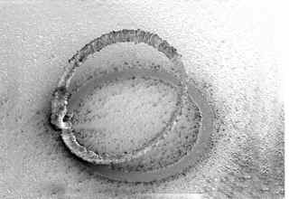
A photonic device fabricated from a novel silica thin film deposited on silicon.
How can we simulate and apply new natural (self-assembly) or non-equilibrium processes to effect atomistic control over the assembly of functional materials which resist the formation of defects and errors or which self-heal under use to create robust engineering systems?
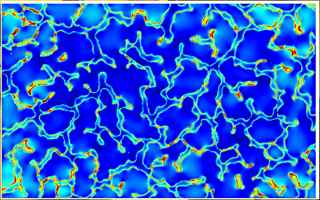
Electromagnetic simulation of a gold island film showing a strong plasmon resonance.
How can we exploit the novel properties of diverse materials in electronic, mechanical, and optical systems through novel integration and synthesis processes to enhance the capabilities of electronic and photonic devices, circuits and systems that can be scaled up for production?How can we simulate and apply new natural (self-assembly) or non-equilibrium processes to effect atomistic control over the assembly of functional materials which resist the formation of defects and errors or which self-heal under use to create robust engineering systems?
How can we best design and engineer materials at the atomistic scale and the electronic and photonic devices fabricated from them to be intimately integrated with living systems so as to enhance the performance of biological systems, to monitor health, to repair defects and to cure diseases?
Published on December 9th, 2016
Last updated on April 9th, 2020