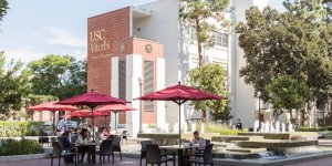
Aerial view of USC ISI/photo credit: USC ISI
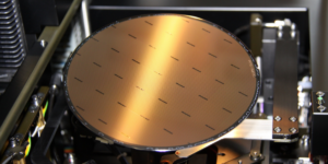
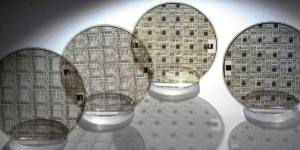
USC Viterbi’s Information Sciences Institute (ISI) and the Intel Corporation’s custom foundry organization today announced a collaboration to design, fabricate and package integrated circuits (ICs) through USC ISI’s MOSIS unit.
The collaboration combines MOSIS’s industry-leading integrated circuit manufacturing expertise with Intel’s high-performance complementary metal-oxide semiconductor (CMOS) fabrication and packaging technology. It positions ISI and Intel Custom Foundry (ICF) to lead a new era of high-performance microelectronic manufacturing for the U.S. and global IC community.
“This is a significant event for the U.S. microelectronics community,” said MOSIS co-director John Damoulakis. “For the first time, the U.S. Government, R&D laboratories, companies, and academia will have access to Intel’s advanced fabrication and packaging technologies economically through MOSIS.”
MOSIS will offer multi-project-wafer runs for prototype integrated circuits, as well as dedicated runs for low-volume production.
“The Intel-supported ecosystem will undoubtedly contribute significantly to microelectronics resurgence and innovation in the U.S.,” said MOSIS co-director James Whalen.
ISI’s Interim Director Craig Knoblock echoed this statement: “There is intense, heavily-funded microelectronics activity in the Asian-Pacific region, and unless the U.S. offers the right ecosystem to innovators, there is a danger that the U.S. may fall behind in the next generation of electronic products and applications.”
ICF’s Vice President Kapil Wadhera added: “The collaboration between Intel and MOSIS ensures that U.S. innovators have at their disposal proper IC design and fabrication technologies to rapidly and cost effectively realize their inventions for the U.S. industrial base, and to compete with their counterparts across the globe.”
About the Technology
The ICF-MOSIS collaboration involves the use of Intel’s 22nm CMOS FinFET (e.g., 22FFL) technology to fabricate either digital or analog/mixed-signal (AMS) ICs for a variety of applications spanning the digital and RFCMOS domains.
Intel’s 22FFL technology is a unique 22nm FinFET process optimized for logic, RF and millimeter wave applications supporting superior performance to planar technologies with both ft and fmax above 300 GHz and 450 GHz. The technology combines high-performance, ultra- low-power logic, RF transistors, and single-pattern back-end flow.
Ultra-low-power logic devices have been developed reducing bit cell leakage by 28X compared to regular SRAM 6T cells. Intel’s 22nm FinFET technology comes with many different options for IC design and fabrication. This technology is designed to accommodate a variety of applications, which often require different overall performance characteristics.
MOSIS’s customers would not only have access to Intel’s advanced fabrication, but also to Intel’s advanced packaging technologies.
About USC Viterbi School of Engineering
Engineering began at the University of Southern California in 1905. Nearly a century later, in 2004, the school was named the USC Viterbi School of Engineering, honoring alumnus Andrew J. Viterbi, inventor of the Viterbi algorithm, a key to cell phone technology and numerous data applications. The school is consistently ranked among the top engineering programs in the world. It enrolls more than 7,000 undergraduate and graduate students, taught by 188 tenured and tenure-track faculty, with more than 90 endowed chairs and professorships. The school offers comprehensive programs in all major areas of engineering, from aerospace and astronautical engineering, to biomedical, chemical, civil and environmental engineering, to computer science and materials science, and to electrical engineering, industrial and systems engineering and mechanical engineering. With annual research expenditures exceeding $207M, the school is home to the Information Science Institute and more than 45 other research centers. Its more than 50,000 alumni span the globe. USC Viterbi is also home to the pioneering distance learning program DEN@Viterbi, ranked as the top such program in the nation the last two years. USC Viterbi is the only engineering school in the nation with three top-10 USNWR rankings: Best Graduate Schools, Best Online Graduate Engineering Programs, and Best Online Information Technology Programs.
Published on May 30th, 2019
Last updated on June 3rd, 2019
