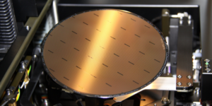


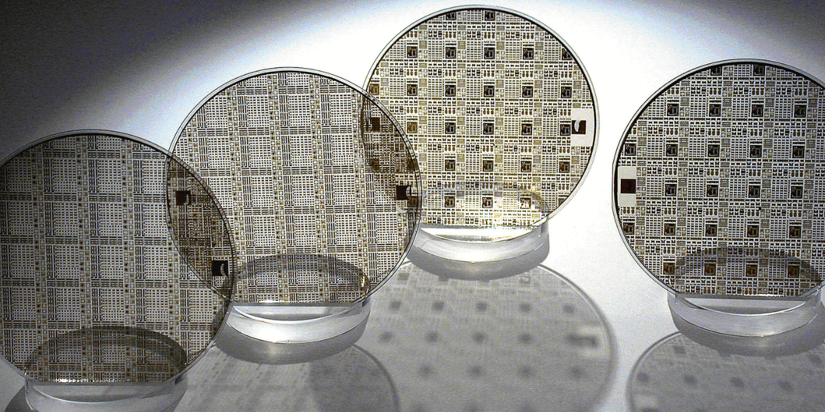
Credit: WIN Semiconductors
The MOSIS Service of Information Sciences Institute, University of Southern California today announced the opening of MPW plan of the Gallium Nitride (GaN) NP15-00 and Gallium Arsenide (GaAs) PQH1-0P processes fabricated by WIN Semiconductors Corp. MOSIS will organize and assemble four designs in a quarter of GaN NP15-00 MPW wafer. MOSIS will also organize and assemble four designs in a quarter of GaAs PQH1-0P MPW wafer. The MOSIS Service starts to process customer’s requests on the MPW runs today. The MOSIS Service and WIN Semiconductors will coordinate the MPW tapeout schedules with the customers. The MOSIS Service provides PDK and other supports to achieve successful tapeouts for the customers.
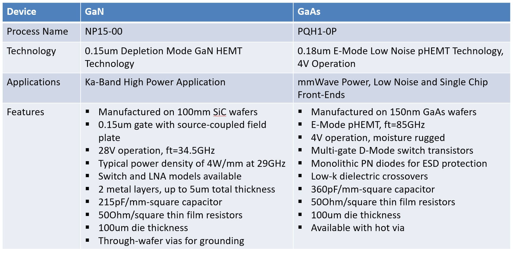
The GaN NP15-00 process enables high power application with frequency range in the Ka band. The GaAs PQH1-0P process enables applications including milli-meter wave power, low noise designs, and single chip front-end, etc. In both the MPW projects, MOSIS supports designs with the fixed size of 4mm x 5.25mm. The summary of the process features of NP15-00 and PQH1-0P are listed in the table below:
 Interested customers can enter your request at MOSIS’ website (www.themosisservice.com). The period of processing customer request starts immediately and will end on July 16, 2023. The MOSIS Service will process necessary account, legal, and financial documents prior to starting the design cycle. If the customer has a packaging plan for the dies, The MOSIS Service can facilitate packaging with experienced vendors.
Interested customers can also directly contact MOSIS in an email (lchang@mosis.com) for further questions.
Published on June 5th, 2023
Last updated on June 2nd, 2023